- 您现在的位置:买卖IC网 > Sheet目录2005 > LTC2175IUKG-14#TRPBF (Linear Technology)IC ADC 14BIT 125MSPS QUAD 52QFN
LTC2175-14/
LTC2174-14/LTC2173-14
22
21754314fa
applicaTions inForMaTion
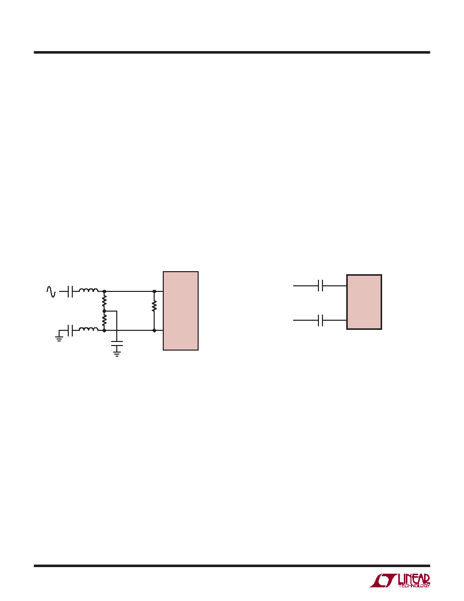
The differential encode mode is recommended for sinu-
soidal, PECL, or LVDS encode inputs (Figures 12 and 13).
The encode inputs are internally biased to 1.2V through
10k equivalent resistance. The encode inputs can be taken
above VDD (up to 3.6V), and the common mode range is
from 1.1V to 1.6V. In the differential encode mode, ENC–
should stay at least 200mV above ground to avoid falsely
triggering the single-ended encode mode. For good jitter
performance ENC+ should have fast rise and fall times.
Thesingle-endedencodemodeshouldbeusedwithCMOS
encode inputs. To select this mode, ENC– is connected
to ground and ENC+ is driven with a square wave encode
input. ENC+ can be taken above VDD (up to 3.6V) so 1.8V
to3.3VCMOSlogiclevelscanbeused.TheENC+threshold
is 0.9V. For good jitter performance ENC+ should have fast
rise and fall times.
Clock PLL and Duty Cycle Stabilizer
The encode clock is multiplied by an internal phase-locked
loop (PLL) to generate the serial digital output data. If the
encode signal changes frequency or is turned off, the PLL
requires 25s to lock onto the input clock.
A clock duty cycle stabilizer circuit allows the duty cycle
of the applied encode signal to vary from 30% to 70%.
In the serial programming mode it is possible to disable
the duty cycle stabilizer, but this is not recommended. In
the parallel programming mode the duty cycle stabilizer
is always enabled.
Figure 13. PECL or LVDS Encode Drive
Figure 12. Sinusoidal Encode Drive
50
100
0.1F
T1
T1 = MA/COM ETC1-1-13
RESISTORS AND CAPACITORS
ARE 0402 PACKAGE SIZE
50
LTC2175-14
217514 F12
ENC–
ENC+
ENC+
ENC–
PECL OR
LVDS
CLOCK
0.1F
217514 F13
LTC2175-14
发布紧急采购,3分钟左右您将得到回复。
相关PDF资料
LTC2202IUK#TRPBF
IC ADC 16-BIT 10MSPS 48-QFN
LTC2205IUK-14#PBF
IC ADC 14BIT 65MSPS 48-QFN
LTC2207IUK-14#PBF
IC ADC 14BIT 105MSPS 48-QFN
LTC2220IUP-1#TRPBF
IC ADC 12BIT 185MSPS 64-QFN
LTC2221IUP#TRPBF
IC ADC 12-BIT 135MSPS 64-QFN
LTC2222IUK-11#TRPBF
IC ADC 11BIT 105MSPS SAMPL 48QFN
LTC2223IUK#TRPBF
IC ADC 12BIT 80MSPS SAMPLE 48QFN
LTC2224IUK#TRPBF
IC ADC 12BIT 135MSPS SAMPL 48QFN
相关代理商/技术参数
LTC2175IUKG-14PBF
制造商:LINER 制造商全称:Linear Technology 功能描述:14-Bit, 125Msps/105Msps/80Msps Low Power Quad ADCs
LTC2175IUKG-14TRPBF
制造商:LINER 制造商全称:Linear Technology 功能描述:14-Bit, 125Msps/105Msps/80Msps Low Power Quad ADCs
LTC2180
制造商:LINER 制造商全称:Linear Technology 功能描述:12-Bit, 65Msps/ 40Msps/25Msps Low Power Dual ADCs
LTC2180CUP#PBF
制造商:Linear Technology 功能描述:ADC Dual 25Msps 16-bit Parallel/Serial (SPI)/LVDS 64-Pin QFN EP 制造商:Linear Technology 功能描述:IC ADC 16BIT DUAL PAR/SRL 64QFN 制造商:Linear Technology 功能描述:ADC 2CH 16BIT 25MSPS QFN-6 制造商:Linear Technology 功能描述:ADC, 2CH, 16BIT, 25MSPS, QFN-64 制造商:Linear Technology 功能描述:ADC, 2CH, 16BIT, 25MSPS, QFN-64; Resolution (Bits):16bit; Sampling Rate:25MSPS; Supply Voltage Type:Single; Supply Voltage Min:1.7V; Supply Voltage Max:1.9V; Supply Current:43.5mA; Digital IC Case Style:QFN; No. of Pins:64 ;RoHS Compliant: Yes
LTC2180CUP#PBF-ES
制造商:Linear Technology 功能描述:ADC Dual 25Msps 16-bit Parallel/Serial (SPI)/LVDS 64-Pin QFN EP
LTC2180CUP#TRPBF
制造商:Linear Technology 功能描述:ADC Dual 25Msps 16-bit Parallel/Serial (SPI)/LVDS 64-Pin QFN EP T/R 制造商:Linear Technology 功能描述:IC ADC DUAL 16BIT 25MSPS 64-QFN
LTC2180CUP#TRPBF-ES
制造商:Linear Technology 功能描述:ADC Dual 25Msps 16-bit Parallel/Serial (SPI)/LVDS 64-Pin QFN EP T/R
LTC2180IUP#PBF
制造商:Linear Technology 功能描述:ADC Dual 25Msps 16-bit Parallel/Serial (SPI)/LVDS 64-Pin QFN EP 制造商:Linear Technology 功能描述:IC ADC 16BIT DUAL PAR/SRL 64QFN